At INO, we specialize in developing solutions designed to make businesses more competitive, no matter what their size or area of activity. From consultation to production, we offer fast lead times and share the risks associated with technology development.
INO’s high power and high speed 3D profilers are designed to measure surfaces several meters wide with unprecedented accuracy in full sunlight. To this end, INO develops a series of dedicated software and hardware tools. Features are offered “à la carte” to speed up the product development cycle and deliver performance.
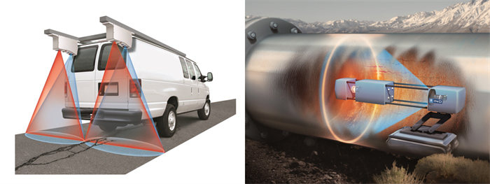
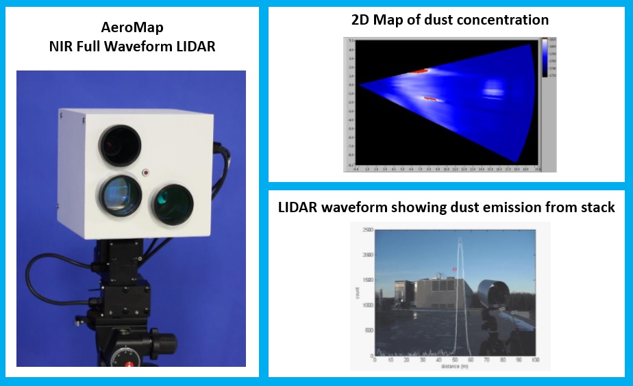
Lidar (light detection and ranging) is the leading optical technology for measuring distances, from a few meters to several kilometers. Like radar, it measures the travel time of light backscattered or reflected by a target. However, lidar makes it possible to determine distances and map its environment with greater precision.
INO’s industrial fiber laser platform allows users to select arbitrarily shaped pulse waveforms with durations ranging from 1 ns to over 1 µs to address a wide variety of laser materials processes. The energy deposition rate at the workpiece may be further controlled by regulating the temporal pulse shape, using either pulse-on-demand or pulse bursts, thanks to a proprietary MOPA system architecture featuring synchronous pumping. Pulse energy up to the mJ level and peak power in excess of 50 kW are readily achieved with outstanding pulse-to-pulse stability for consistent and precise results.
Fiber Optic Chemical Sensor
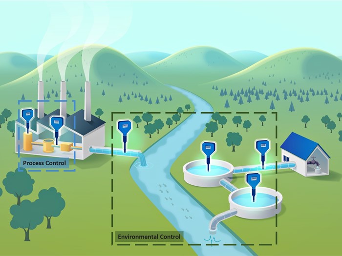
INO has developed a novel fiber optic chemical sensor technology based on ion-selective membranes. This sensor relies on the membrane’s absorption spectrum, which depends on the concentration of a target ion. The membrane is used as the cladding when deposited on a multimode fiber, which guides the signal. The uniqueness of this technology comes from the fact that the concentration of ions in the solution is monitored via evanescent wave spectroscopy. This configuration allows concentration measurements in colored or even opaque solutions, since the light propagating in the core only interrogates the membrane and never “sees” the medium under testing. Moreover, the membrane composition can be adjusted to detect different ions.
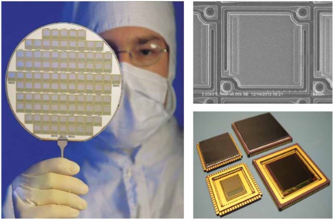
INO offers a complete range of MEMS/MOEMS foundry services. Whether you need a very specific service or a fully-integrated MEMS creation process, we have the resources and expertise to help you reach your goals and deliver results. Our state-of the-art MEMS foundry clean room facility is perfectly adapted to the processing of 6″ and 8″ silicon substrates.
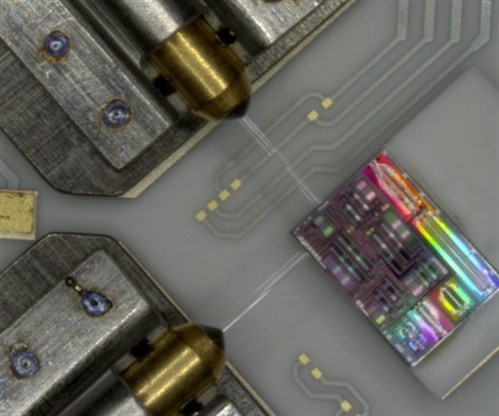
Silicon Photonics Packaging
Packaging accounts for a gigantic part of silicon photonics devices’ overall cost. Thanks to more than 20 years of experience in multiple packaging applications, INO can assume this critical challenge. We build custom silicon photonics packages that will meet your specifications.